Solar Wafer M12 M10 M9 M6 G1 M4 M2
Feb 23, Solar wafer size evolvement In order to increase the power of solar panels and reduce the cost of solar panels, the silicon wafer industry
Flexible silicon solar cells with high power-to-weight ratios
Jan 31, A study reports a combination of processing, optimization and low-damage deposition methods for the production of silicon heterojunction solar cells
The relationship between the weight and the power of solar
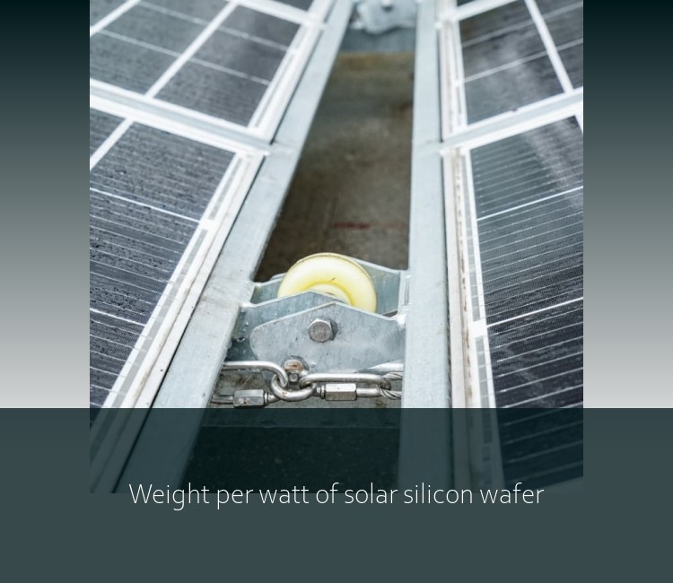
The thickness of the silicon wafer is unchanged and the weight is unchanged:156*156,8 inch polycrystalline silicon chip efficiency reached 16%, single-chip power of 3.89W.This can be
400W Solar Modules A Complete Guide to Costs, Efficiency,
The weight per wafer increases from 27g for 182mm to 38g (40% more silicon material used), but because it can be cut into more cells, the cost per watt of the silicon wafer actually drops from
Solar Silicon Wafer Size M0 M2 G1 M6 M10
Jan 8, What do "M" and "G" stand for in solar wafer size? It begins with the letter "G", which means that the solar silicon wafer is full square
How Many Watts of Silicon Wafers Power Your Photovoltaic
Let’s start with a tasty metaphor: silicon wafers in solar panels are like pizza slices – their size, thickness, and quality determine how much energy you get. But instead of calories, we’re
Trends of Solar Silicon Wafer Size and
Mar 31, The PV industry has been rapidly evolving with advancements in wafer size, wafer thickness, and solar cell technologies. These
Photovoltaic panel silicon wafer content requirements
to 200mm, d slice of silicon in crystalline form (silicon wafer). Silicon has an energy band g operational life is 20-30 years at least [7, 13, 16]. Based on these values, at a bare minimum,
Photovoltaic panel silicon wafer size standard
Before ,monocrystalline silicon wafers were dominated by 125mm x 125mm width (165mm silicon ingot diameter) and only a small number at 156mm x 156mm(200mm silicon ingot
Wafer calculator
May 16, Welcome to the wafer calculator The user selects (i) the shape and dimensions of a wafer, (ii) the wafer material (e.g., Si, GaAs), and (iii) the conversion efficiency at a particular
Solar Wafer M12 M10 M9 M6 G1 M4 M2
Feb 23, Solar wafer size evolvement In order to increase the power of solar panels and reduce the cost of solar panels, the silicon wafer industry has been driven to continuously
Solar Silicon Wafer Size M0 M2 G1 M6 M10 G12 and What
Jan 8, What do "M" and "G" stand for in solar wafer size? It begins with the letter "G", which means that the solar silicon wafer is full square Beginning with the letter "M", it means
Trends of Solar Silicon Wafer Size and Thickness for Different
Mar 31, The PV industry has been rapidly evolving with advancements in wafer size, wafer thickness, and solar cell technologies. These developments aim to optimize conversion
Photovoltaic panel silicon wafer size standard
Before ,monocrystalline silicon wafers were dominated by 125mm x 125mm width (165mm silicon ingot diameter) and only a small number at 156mm x 156mm(200mm silicon ingot
Evolution of Silicon Wafer Size
Jan 14, As the size of a single silicon wafer increases, the number of cells in a single solar module decreases, the number of silicon wafers decreases accordingly, and the effective light
Photovoltaic panel silicon wafer size standard
Before ,monocrystalline silicon wafers were dominated by 125mm x 125mm width (165mm silicon ingot diameter) and only a small number at 156mm x 156mm(200mm silicon ingot
Optimal Module Solution for Achieving Lower LCOE of
Jun 17, In early time, PV cells are similar to semiconductor chips, and the equipment and process costs are relatively high. Thus, increasing the size of silicon wafer can significantly
The solar cell wafering process
May 21, Another relevant field of research is the reduction of the wafer thickness in order to produce more wafers per kilogram silicon.
Photovoltaics Report
Nov 5, Silicon wafer-based technology accounted for about 98% of total production in with a 70% share of n-type wafers according to ITRPV. Monocrystalline technology became
Silicon Wafer Production and Specifications
Jul 12, Polishing After etching, both wafer surfaces appear like the rear side of fi nished sin-gle-side polished wafer. In order to attain the su-per-fl at, mirrored with a remaining surface
Silicon to Solar
Solar value chain and conversion steps from metallurgical silicon (mg-Si) to solar module inese companies. The long-term Chinese commitment to establishing a domestic solar industry has
Polysilicon | Solar Value Chain
Polysilicon is used to manufacture crystalline wafers for solar modules. 25% of the cost of a crystalline module is just for polysilicon. The industry is plagued by lower demand and
A global statistical assessment of designing silicon-based solar
Jun 19, Here, we first visualize the achievable global efficiency for single-junction crystalline silicon cells and demonstrate how different regional markets have radically varied
Why are monocrystalline wafers increasing in size?
May 21, After , 156mm × 156mm wafers increasingly became the popular choice (lower cost per watt) for p-type mono and multi wafer sizes.
Analysis of development of high-power
Jul 7, Seven companies, including LONGi, Jinko Solar, JA Solar, and Canadian Solar jointly released the M10 (182mm) monocrystalline silicon
Wafer (electronics)
In electronics, a wafer (also called a slice or substrate) [1] is a thin slice of semiconductor, such as a crystalline silicon (c-Si, silicium), used for the fabrication of integrated circuits and, in
What is the cost of silicon solar cell?
The silicon wafer itself—the thin slice of crystal—accounts for approximately 56% of the total cost of a finished solar cell. This makes the wafer the
Photovoltaics Manufacturing, Polysilicon | Solar Power
Silicon ribbons: This is a continuous process whereby thin ribbons or sheets of multicrystalline silicon are drawn from a polysilicon melt. The subsequent cutting into wafers does not produce
Solar price trend
Inventory: Wafer inventory has now surged to over 21 GW, a relatively high level. Growing bearish sentiment toward future prices has dampened downstream procurement willingness, hindering
PV spot price
6 days ago InfoLink Consulting provides weekly updates on PV spot prices, covering module price, cell price, wafer price, and polysilicon price. Learn about photovoltaic panel price trends
How many watts does a solar panel wafer
Sep 21, To appropriately evaluate how many watts a solar panel wafer generates, it is crucial to assess the entire solar setup, including inverter
LONGi Solar-Silicon Wafer Price
2 days ago Here is the latest silicon price information for your reference.
Wafer calculator
May 16, Welcome to the wafer calculator The user selects (i) the shape and dimensions of a wafer, (ii) the wafer material (e.g., Si, GaAs), and (iii) the conversion efficiency at a particular
Technical Discussion & Message Board
Share your thoughts on residential solar technology and home energy storage systems. Comments saved locally (demo).